
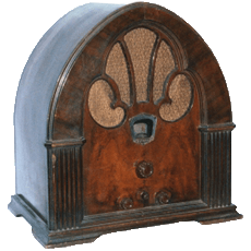


02-11-2026, 11:31 PM
Work has been busy lately, but I think we're about caught up! Anyway, progress has been intermittent on the electrical restoration lately, but I'm about set up to get it in motion.
I've been working on a design for a new multisection cap for C102. I had so much fun designing PCB replacements for the top-of-chassis mounted multisection caps for my 46-480 that I figured I would do it again here for the 48-482. There's three multisection caps this time around, but only one is mounted on top of the chassis. It's a twist-lock style, like one of the two I had designed for the 46-480 last year.
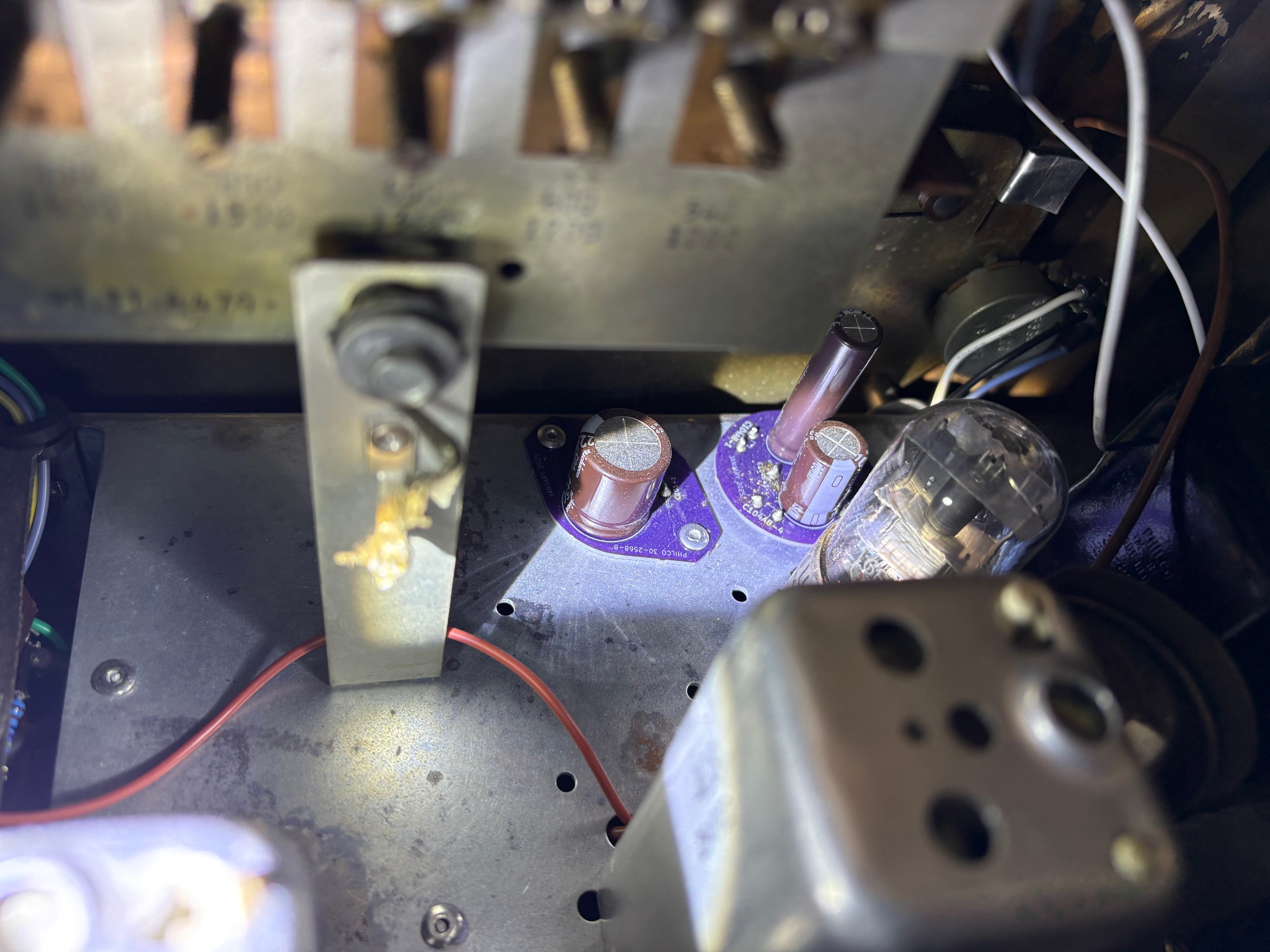
Essentially, I followed the same process with the lessons learned on those two prior designs. However, this new PCB came with a challenge of it's own--for this new C102 capacitor (Philco part number 30-2570-1), there are three capacitors stuffed inside the can: a 10uF, a 15uF, and a 30uF capacitor. They all share a common negative. I found some high-hour Nichicon electrolytics for my new design (had to substitute a 33uF for the original 30uF), but the 33uF capacitors have a sizeable footprint. In fact, it's a bit bigger than a third of the real estate of the 1.5" diameter disc of a PCB. I couldn't find any way to place all three through-hole mount caps on top of the PCB with through-hole solder lugs on the underside and the same four quick-connect lugs I used previously for the twist-lock tabs.
I ran through SEVERAL iterations of the design, but here's what I settled on. Fair warning, but it is absolutely over-engineered. I'm okay with that, though. Something is very fun about designing a rugged part to install within the exact slot of the original capacitor.
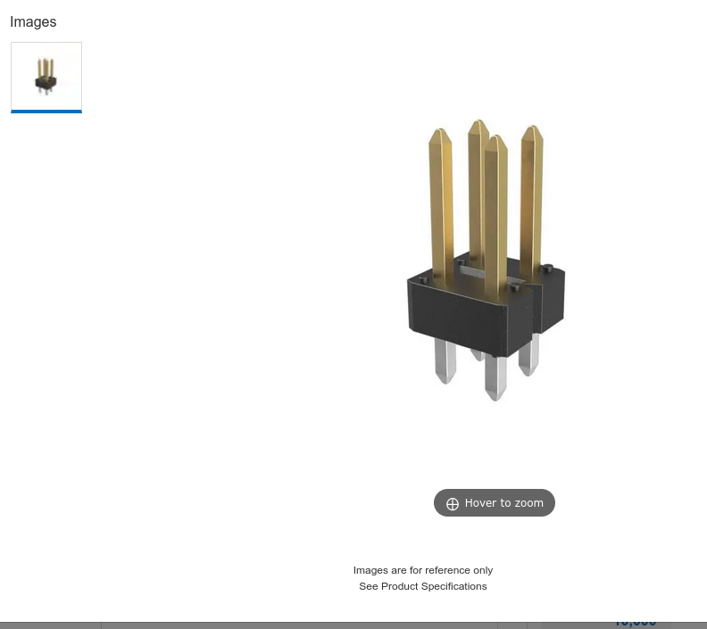
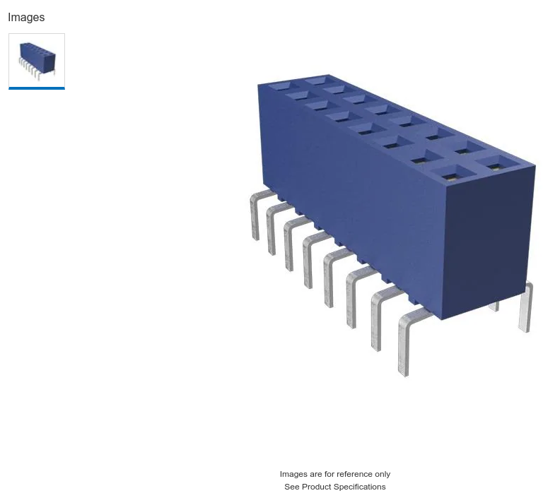
I decided to design two PCBs, a lower and an upper. Because of the total footprint of the caps, I also needed to change from a circular PCB outline to a square (same tab locations, so it will still click right into the chassis; there are also no interferences on the chassis for fitting a square PCB in this space). The lower board would be used for the solder lugs for each of three capacitors' positive connections and for the four quick connect lugs used for the twist-lock tabs. These four tabs are connected to the common negative of the capacitors. The upper PCB, in turn, will have all three capacitors mounted on its top side. To connect the two layers of PCB, I needed a solution with a minimal footprint. I came up with a 2x2 header and receptacle (photos below; notice that the receptacle photo shows a sample with more connections than the 2x2, but it is merely a representative photo from Mouser).
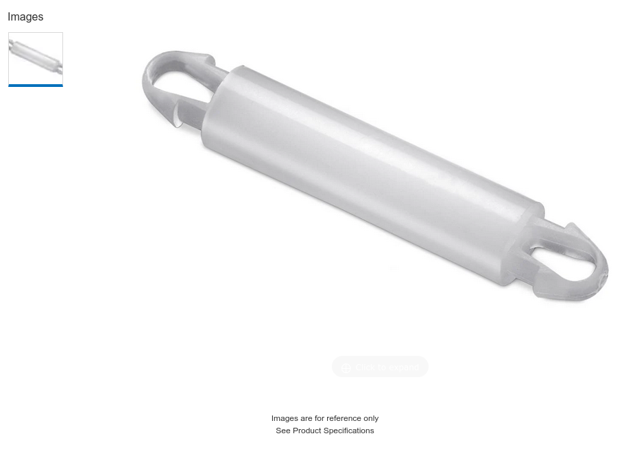
This combination of header and receptacle provides secure electrical connection between the two PCBs, but what about secure structural connection? To solve that, I designed through holes for spacers:
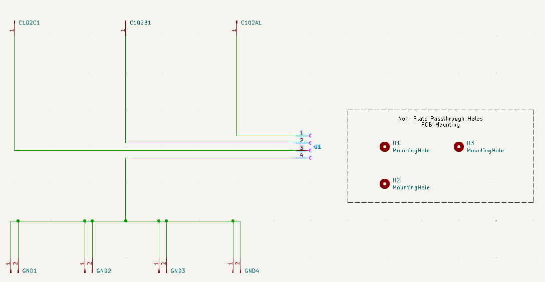
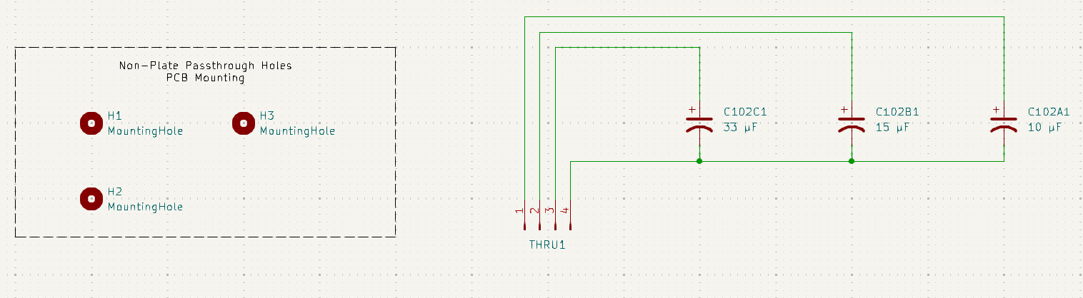
And here is the resultant product. We'll start with lower and upper schematics (in that order):
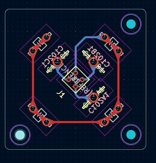
And now the lower and upper PCB outlines (in that order):
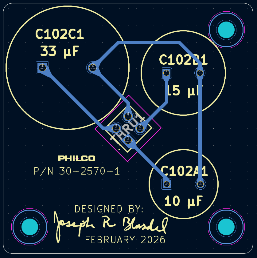
And, now for top and bottom views of the lower PCB:
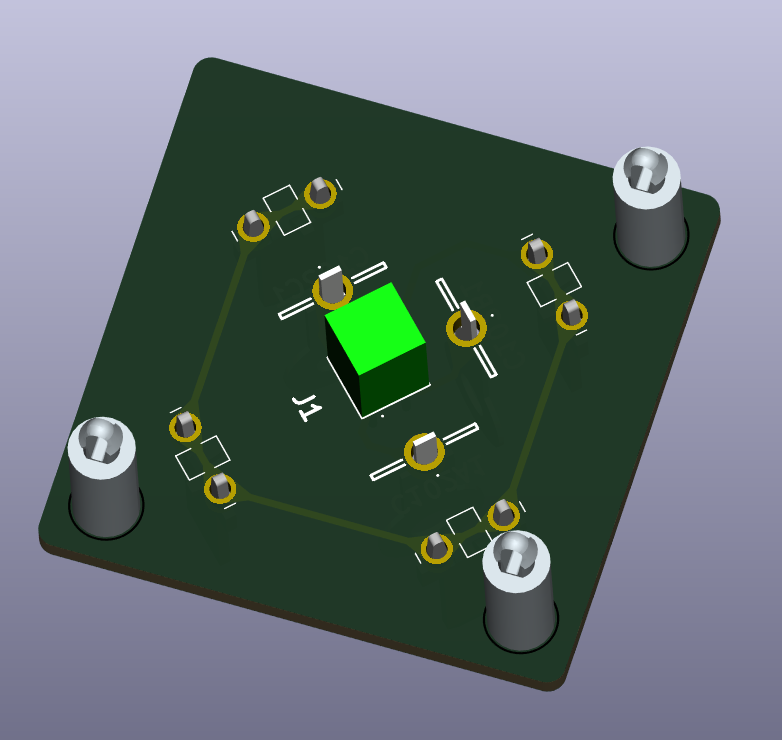
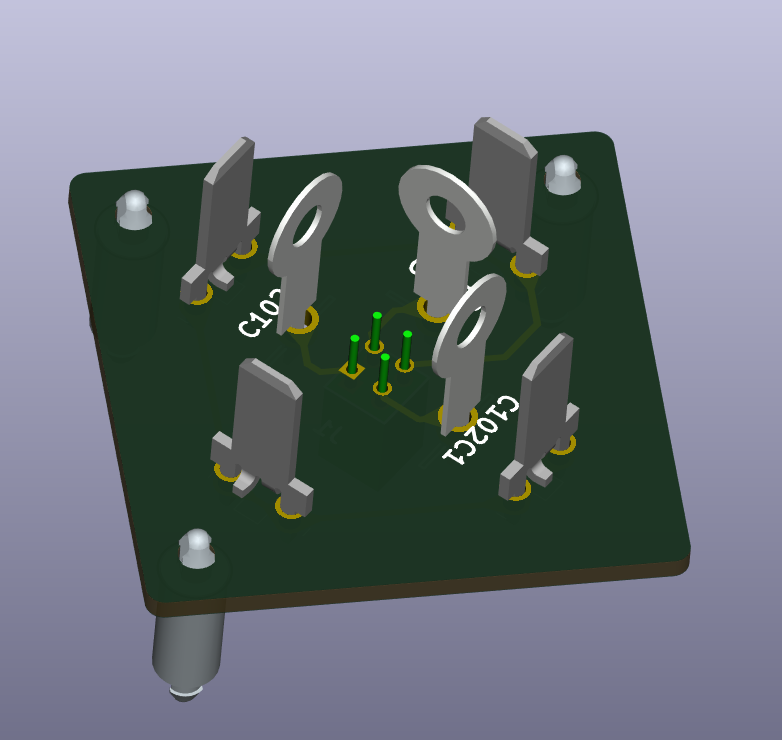
And, finally, top and bottom views of the upper PCB:
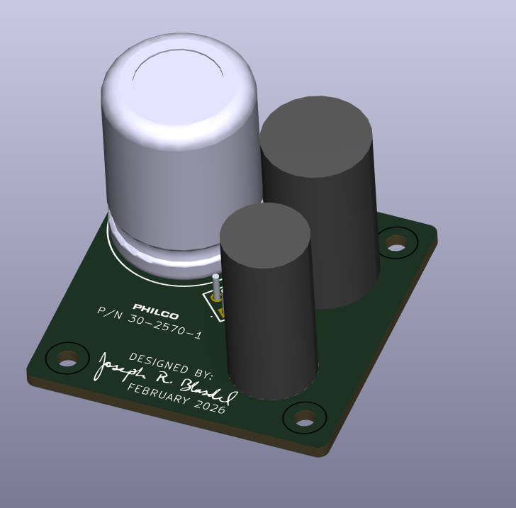
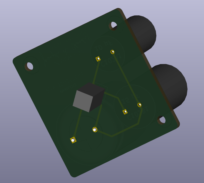
I learned a few new tricks that I've implemented on this one. One trick was the conversion of images into silkscreen graphics. You'll notice that the "PHILCO"on the top PCB is stylized per the PHILCO logo. I also added my signature so that someone eighty years from now will know who wasted their time designing this part.
Now for the important calculations.
- Trace width: I went with 0.5mm. This is an 80W radio.The caps operate at 250VDC; assuming (conservatively) that all current will pass through any one capacitor, that gives us a current of 0.32A. This equated to a trace width of just shy of 0.2mm. I had the space for it, so I went with 0.5mm. Never hurts to upsize traces on these power supply components. I also added tear drops.
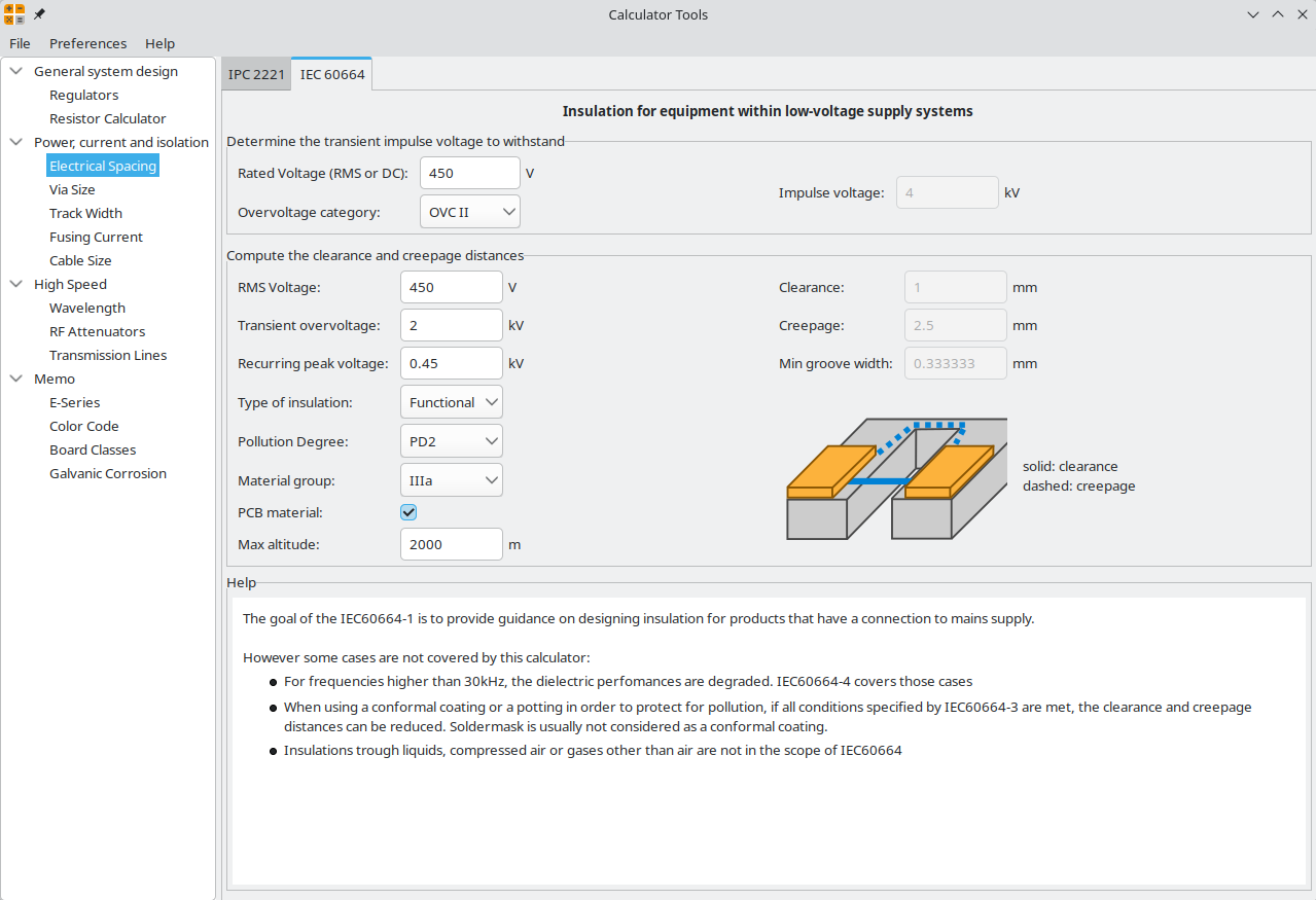
- Minimum creepage and clearance: I designed for 450VDC (the original cap is rated for 450VDC). For the rest of the parameters in the calculation tool, I made the same conservative assumptions I detailed in my cap design summary for the 46-480. All traces and components meet these requirements.
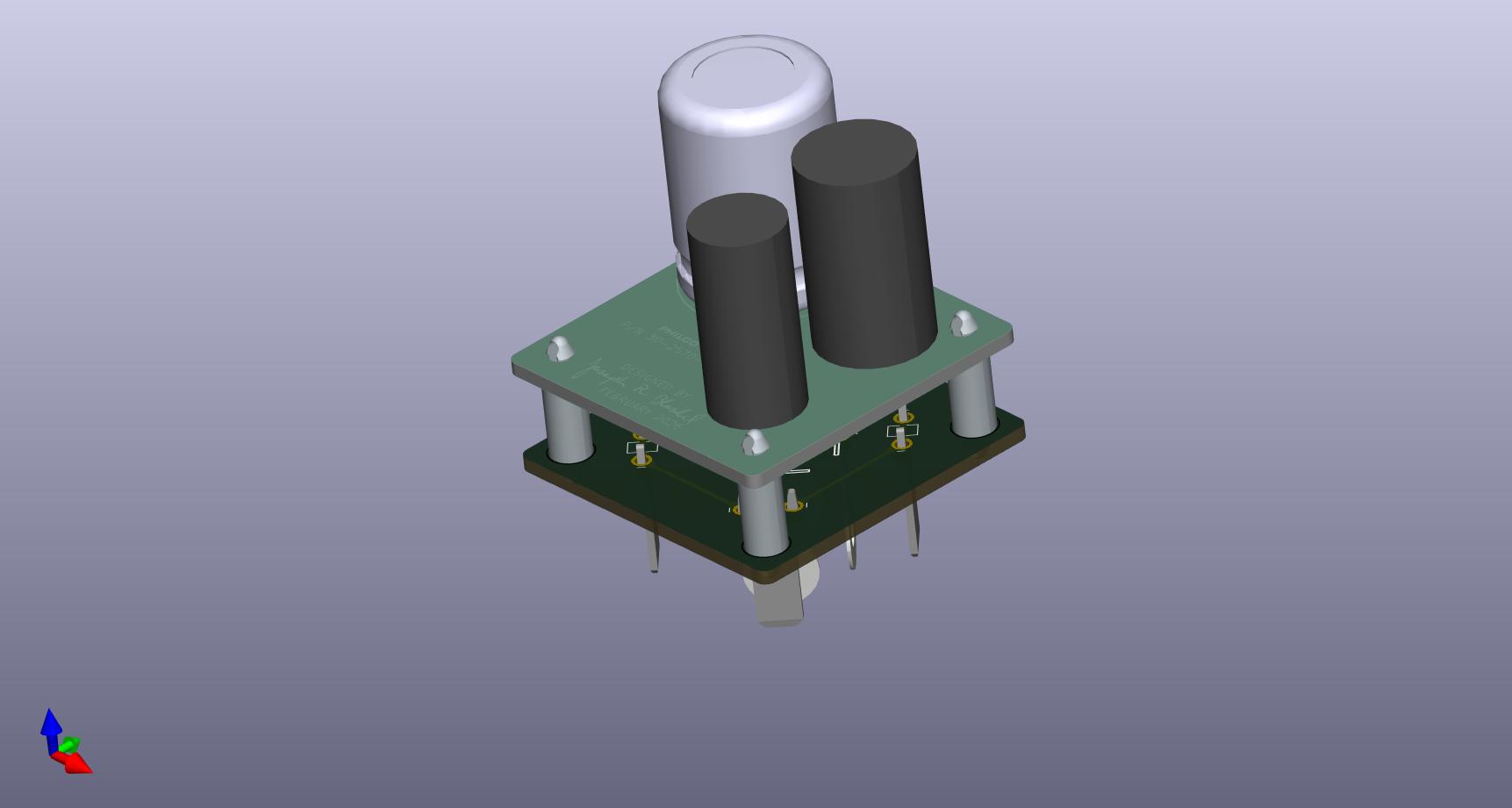
Here's a mockup of the full assembly:
I've been working on a design for a new multisection cap for C102. I had so much fun designing PCB replacements for the top-of-chassis mounted multisection caps for my 46-480 that I figured I would do it again here for the 48-482. There's three multisection caps this time around, but only one is mounted on top of the chassis. It's a twist-lock style, like one of the two I had designed for the 46-480 last year.
Essentially, I followed the same process with the lessons learned on those two prior designs. However, this new PCB came with a challenge of it's own--for this new C102 capacitor (Philco part number 30-2570-1), there are three capacitors stuffed inside the can: a 10uF, a 15uF, and a 30uF capacitor. They all share a common negative. I found some high-hour Nichicon electrolytics for my new design (had to substitute a 33uF for the original 30uF), but the 33uF capacitors have a sizeable footprint. In fact, it's a bit bigger than a third of the real estate of the 1.5" diameter disc of a PCB. I couldn't find any way to place all three through-hole mount caps on top of the PCB with through-hole solder lugs on the underside and the same four quick-connect lugs I used previously for the twist-lock tabs.
I ran through SEVERAL iterations of the design, but here's what I settled on. Fair warning, but it is absolutely over-engineered. I'm okay with that, though. Something is very fun about designing a rugged part to install within the exact slot of the original capacitor.
I decided to design two PCBs, a lower and an upper. Because of the total footprint of the caps, I also needed to change from a circular PCB outline to a square (same tab locations, so it will still click right into the chassis; there are also no interferences on the chassis for fitting a square PCB in this space). The lower board would be used for the solder lugs for each of three capacitors' positive connections and for the four quick connect lugs used for the twist-lock tabs. These four tabs are connected to the common negative of the capacitors. The upper PCB, in turn, will have all three capacitors mounted on its top side. To connect the two layers of PCB, I needed a solution with a minimal footprint. I came up with a 2x2 header and receptacle (photos below; notice that the receptacle photo shows a sample with more connections than the 2x2, but it is merely a representative photo from Mouser).
This combination of header and receptacle provides secure electrical connection between the two PCBs, but what about secure structural connection? To solve that, I designed through holes for spacers:
And here is the resultant product. We'll start with lower and upper schematics (in that order):
And now the lower and upper PCB outlines (in that order):
And, now for top and bottom views of the lower PCB:
And, finally, top and bottom views of the upper PCB:
I learned a few new tricks that I've implemented on this one. One trick was the conversion of images into silkscreen graphics. You'll notice that the "PHILCO"on the top PCB is stylized per the PHILCO logo. I also added my signature so that someone eighty years from now will know who wasted their time designing this part.
Now for the important calculations.
- Trace width: I went with 0.5mm. This is an 80W radio.The caps operate at 250VDC; assuming (conservatively) that all current will pass through any one capacitor, that gives us a current of 0.32A. This equated to a trace width of just shy of 0.2mm. I had the space for it, so I went with 0.5mm. Never hurts to upsize traces on these power supply components. I also added tear drops.
- Minimum creepage and clearance: I designed for 450VDC (the original cap is rated for 450VDC). For the rest of the parameters in the calculation tool, I made the same conservative assumptions I detailed in my cap design summary for the 46-480. All traces and components meet these requirements.
Here's a mockup of the full assembly:
Joseph
Philco 39-750 EZ
Philco 46-480
Philco 47-1230
Philco 48-482
Philco 49-906


